
 English
  Polish
 German
↓
Aktualności
Good cooperation with EMS requires mutual commitment
03
gru
2015
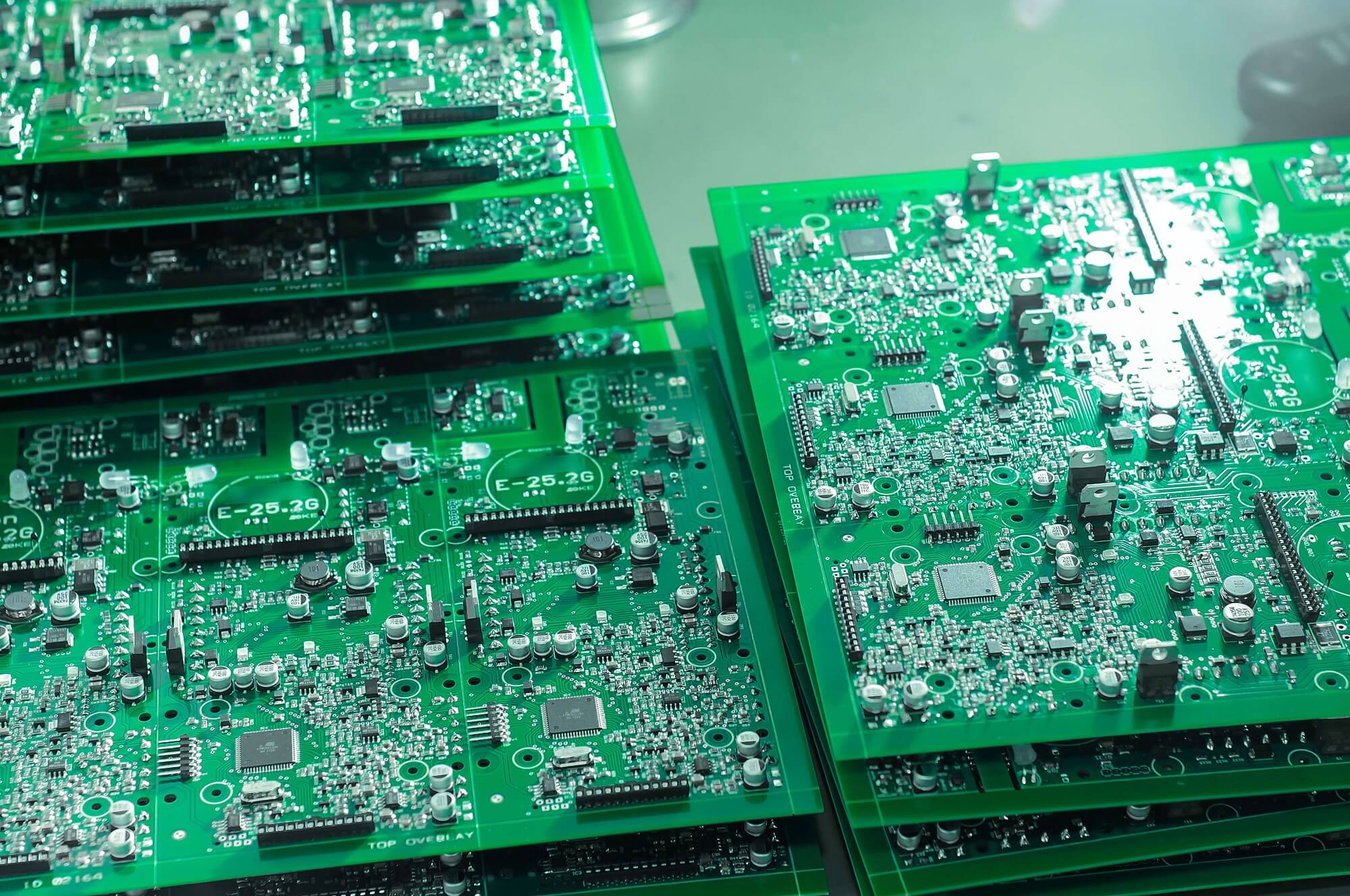
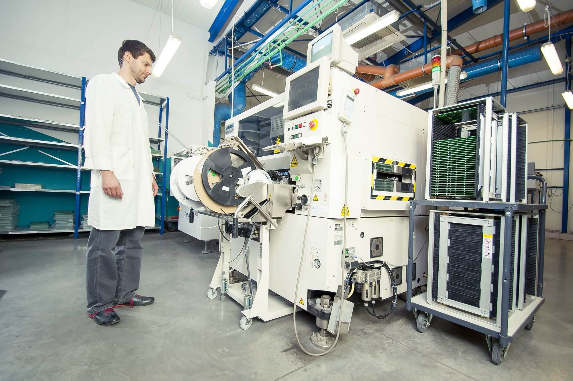
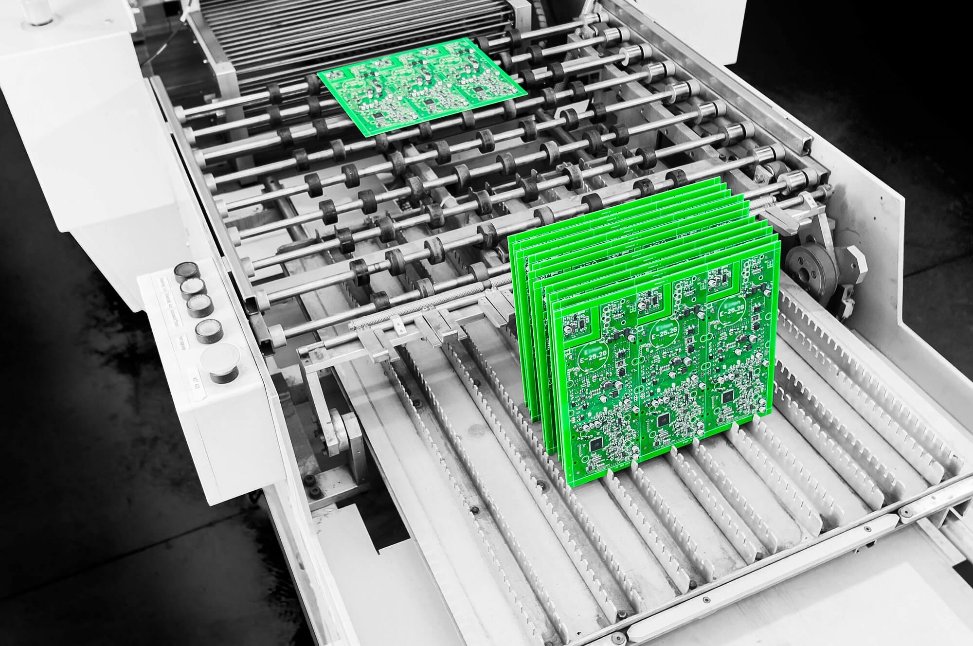
Contract manufacturing of electronics is a service targeted to a wide range of customers, some of which are both specialized manufacturers of electronic devices, as well as companies producing weakly bound electronic devices. Many clients have different knowledge and experience on production technology, uses a variety of design tools and software, but each time hoping that the manufacturer EMS will help in bringing the project to a state where it will meet all the technological requirements. Unfortunately, the consequence of this state, and the chronic lack of time and haste is the increasing number of errors in the manufacturing documentation. They are a source of cost and complexity for all so you should be familiar with the most popular in order to try to avoid them. Here are some of those that we most often we face in everyday work in the Electronic Company.
Margins
Mainly in terms of preserving the technological margin. Machinery imposing a paste and stacking components require the presence of a few millimeters piece of \"clampingu\" (clamp - terminal), located mostly on the long side. It is not needed if the SMT components are more than 5-6 mm from the edge of the board (depending on the machine). So if at the design stage, we can offset PCB SMT components from the edge, let\'s do it, because the addition of margin means a higher cost of production.
Fiducial
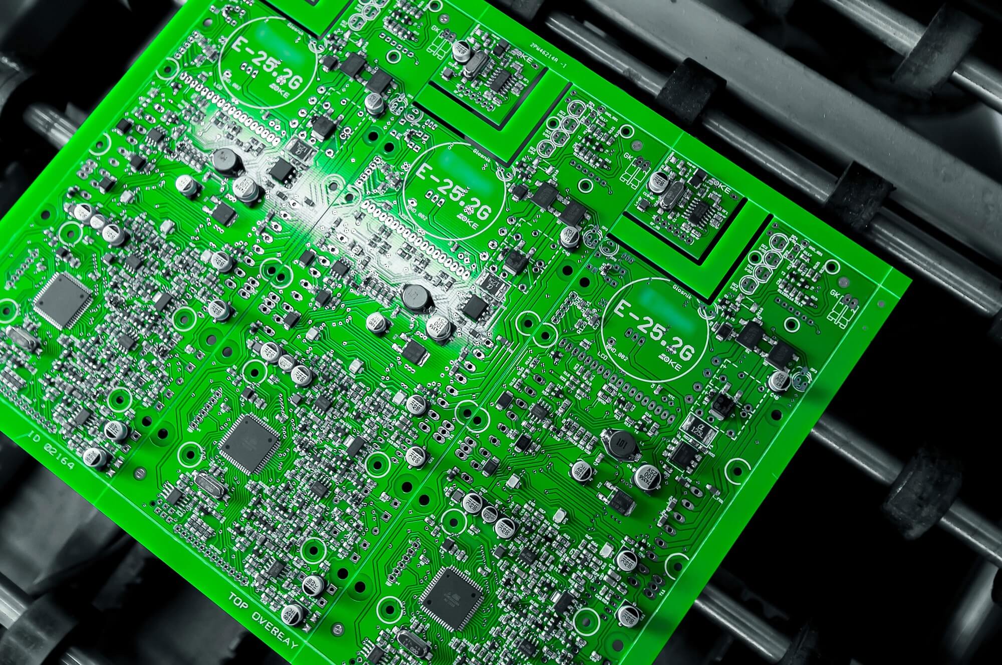
These are reference points that serve the machine to recognize poses mats, defining the reference and position error correction possible. Fiducial are necessary for the smooth SMT. Depending on the equipment used in the form of exposed from the solder mask pad of suitable form, sometimes such openings. Machinery for manual application of the paste. Shapes tags are mostly just dots, squares, crosses. Their sizes range from 1 to 3 mm.
Placing FIDUCIE the project is not necessary, but it is in good taste. If they will not be in the plate itself is a designer during panelizacji likely to add them yourself or ask about them. Maybe they did not do, if the contract amounts only to produce a printed circuit board without installation. Fiducial can of course and place in the contour of the plate. In this case, it is basically part of the mosaic and the matter is resolved reference points. Sometimes, however, the mosaic of the PCB is so densely crammed that it is not possible to add up even a small Fiducial. Then you need to add margins assembly, which are placed Fiducial, just not on the side, which will be \"terminal\" for the then obscure fiducial, or at least within an appropriate distance if we have confidence in the depth clampingu. The other possibility is the abandonment of reference points as separate pads. You can then use sufficiently large grommets or unused pads SMT components.
Why can not I use the pads as such at all? You can as long as the pad is clean. However, SMT component assembly takes place with the applied paste, and this means that pad will have a different color and shape of which is stored in the machine\'s memory and the unit expects to find.
And the last point. How much should be Fiducia on the board? At least two, and preferably three. They should be placed as far as possible diagonally. The higher the diagonal of the more accurate positioning.
Other errors
Often attached to project documentation is a file pick and place. Unfortunately, it is rarely directly helpful to the editor.
Mainly because I often point zero p & p is different from the one that is physically located on the PCB / panel (if at all there). A little better if p & p zero point is the lower left edge of the plate. Unfortunately, the machine using the Fiducia edges of the plates do not detect. Fortunately, in this case, the designer is relatively easy to calculate all coordinates, even though it takes the necessary time. But there are files where the reference point is the center of the planetary system. Then begins an investigation and waiting for a new file with a clarification, of which datum point.
After placing FIDUCIE in the project within the outline of the PCB should generate a file with the coordinates use of the Fiducia, or at least refer to the bottom left edge of the PCB. In the header file, you can enter information about a reference point for the designer.
Pick & Place component in addition to the coordinates of the center (center component, not the center of the pad!) Contains information on the corner. Unfortunately angle definition seldom agree between software design and machine. To have such compliance would prepare the component library as defined angles in the machine. And it would require, first hold a dossier same machine secondly preparation of documentation for a given machine, because not all benefit from the vending machine one manufacturer. The result is a job that does not pay even taken at the design stage. This task falls on the shoulders of the poor editor who must check the compatibility of angles.
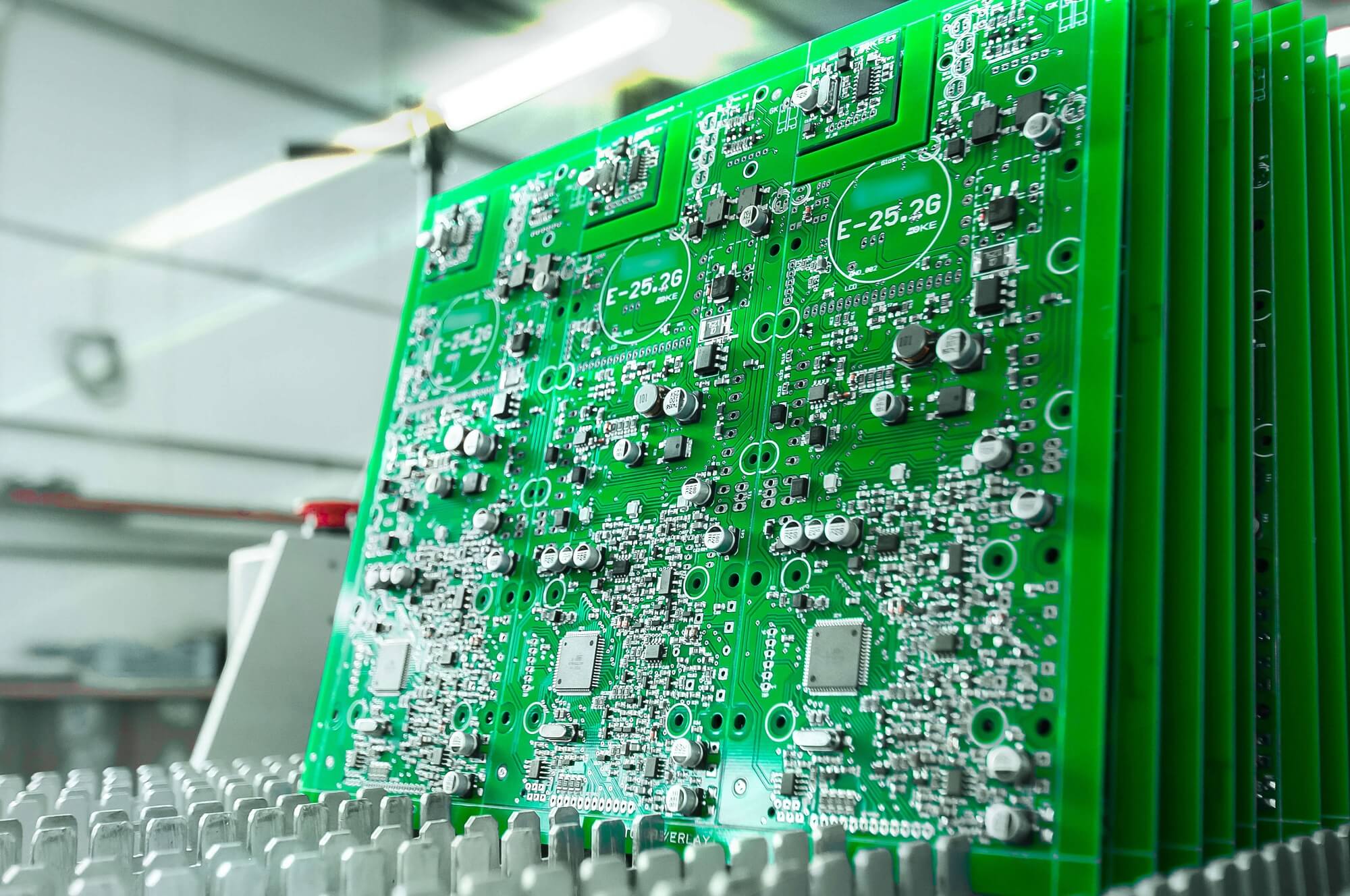
BOM
The most common problem is a lack of detail which leads to the need to improve file. And that means an extension of the entire production process. The table shows an example of how it has to be prepared.
Often, the plate contains elements that are not included in the bill. The designer must guess whether he got a complete BOM, or perhaps some version in between. Most often it turns out that the item has simply can not be mounted. Meanwhile, the BOM is a list of absolutely all the elements. No cast some must be clearly included in it. The good taste is writing in the column next to the list of possible replacements, the use of a spreadsheet, scheduling according to the type of assembly (SMT, THT) and to check the availability of elements in the design phase.
The correct designation of the elements on the plates
The most common mistake is not tying attention by the designers to position the layer descriptive designators. It happens that they are placed on each adapter, the edges of the plates or pads. They will not be physically visible on the PCB. Even if the plate is to be performed without description, it should be to prepare a technical documentation which is based on these descriptions. Sometimes it happens that designators are positioned directly beneath the element through which the fill will not be visible. This is not a problem, provided that this is done on purpose. Sometimes projects, where one element can be filled on one of the two pads. Make sure that the layer Descriptive at this point was clear. It is good to prepare a drawing showing the unequivocal position of the elements depending on the version of the assembly. Note should also be on file describing p & p.
It is also subject to check whether the design of all components that are sensitive to the polarizations have their description that defines their position. It\'s about dots and chops for integrated circuits, arrows or strips for diodes and capacitors, but also correct polarity for connectors, sockets and switches. Here a minor point for the determination of polarization SMT LEDs. Selection in the form of a strip or square that might not be a good idea. It happens that the producers of LEDs apply their mark polarity LED, which is opposite to that assumed in the project. Therefore it is better to select the arrow direction conduction.
The biggest challenge is descriptive designs with dense population. If this is done on the elements 0603 and describing the smaller becomes a chore. Apply the descriptions of the offset, cascading and with reference to the entire area. Remember that a well-prepared documentation is a guarantee correct and efficient installation.
Maciej Bilski, dział projektowy
Kompania Elektroniczna
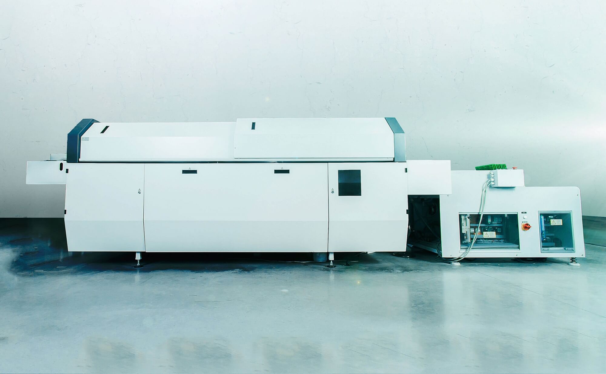
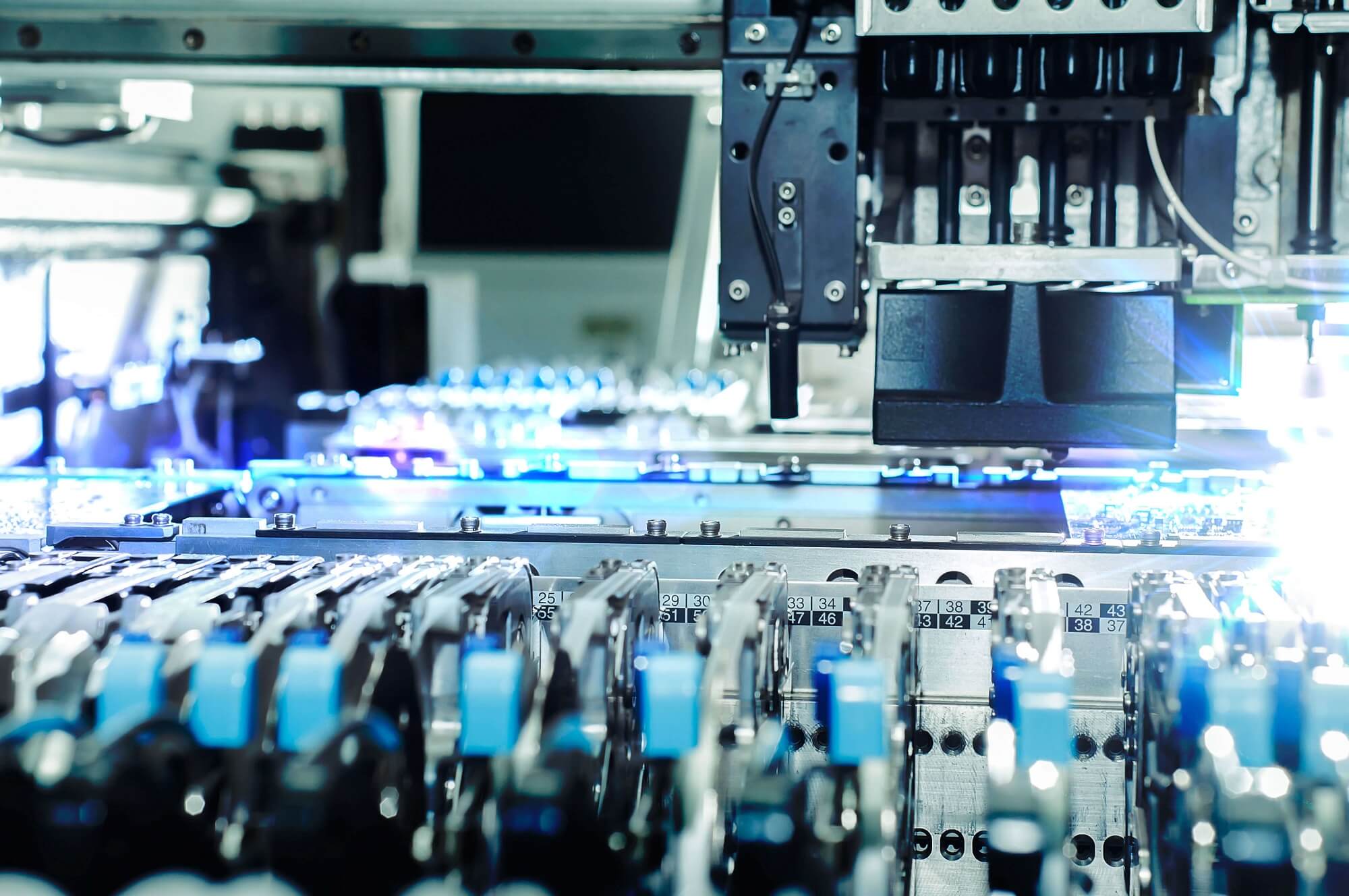
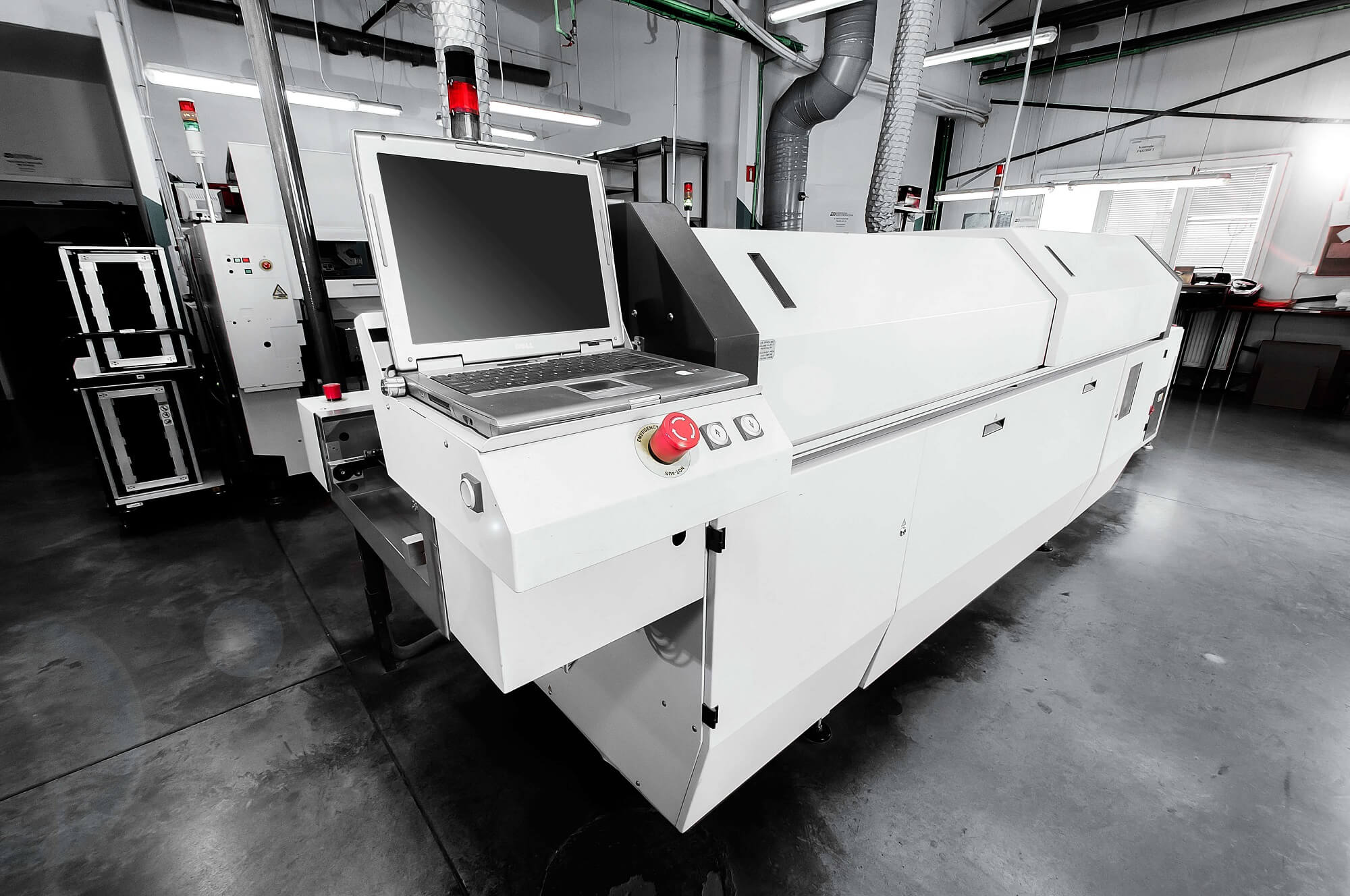
PHOTO GALLERY
Check photo gallery >>
CONTACT
KOMPANIA ELEKTRONICZNA Sp. z o.o.
Printed Circuit Boards - SMT and THT
Assembly - Electronic Components
Warsaw/Raszyn, Poland.
ul. Żwirowa 63, Puchały, 05-090 Raszyn
Sales Office:
ul. Puławska 34 budynek 31, 05- 500 Piaseczno
 |
Tel./fax: +48 22 715 66 06 i 07 |
 |
E-mail: biuro.handlowe@komele.eu |
 |
Skype: KomeleBiuroHandlowe |